In the vast landscape of electronic manufacturing, the process of Printed Circuit Board Assembly (PCBA) stands as a cornerstone, orchestrating the transformation of disparate electronic components into cohesive systems. PCBA entails a meticulous orchestration of various components and steps, each contributing to the creation of functional electronic devices. In this comprehensive guide, we embark on a journey to unravel the intricacies of PCBA assembly, shedding light on the key components and steps that drive modern electronic production.

PCBA assembly embodies the convergence of technology and craftsmanship, seamlessly integrating electronic components onto printed circuit boards (PCBs) to form the backbone of electronic systems. It is a process characterized by precision, efficiency, and reliability, underpinned by a deep understanding of electronic principles and manufacturing techniques. From the inception of the PCB to the final inspection of assembled systems, every facet of the PCBA process plays a pivotal role in shaping the landscape of modern electronics.
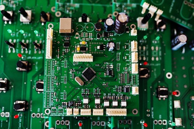
Printed Circuit Board (PCB): At the heart of PCBA lies the printed circuit board, a meticulously engineered substrate that provides the foundation for electronic component integration. PCBs come in various forms, ranging from single-sided to multi-layered configurations, each tailored to accommodate the specific requirements of the electronic system. These boards serve as the conduit through which electrical signals flow, facilitating the seamless interaction of electronic components.
Electronic Components: Central to the PCBA process are the electronic components that populate the surface of the PCB, each contributing to the functionality and performance of the final electronic system. From passive components such as resistors and capacitors to active components like integrated circuits (ICs) and microprocessors, the assembly of these components forms the essence of PCBA. Their strategic placement and precise soldering are paramount to the reliability and functionality of the assembled system.
Solder Paste: Solder paste serves as the adhesive that binds electronic components to the surface of the PCB, forming robust electrical connections essential for the operation of the electronic system. Comprising a precise blend of solder alloy and flux, solder paste is carefully applied to designated areas of the PCB through a process known as stencil printing. Its controlled deposition ensures optimal soldering during the reflow soldering process, facilitating the creation of durable and reliable solder joints.
1. PCB Fabrication:
The journey of PCBA begins with the fabrication of the printed circuit board, a process characterized by precision and attention to detail. PCB fabrication involves a series of intricate steps, including substrate preparation, copper layer deposition, photoresist application, etching, and surface finishing. These processes culminate in the creation of a pristine PCB, meticulously crafted to accommodate the electronic components that will populate its surface.
2. Component Placement:
With the PCBs in hand, the next step in the PCBA process is component placement, where electronic components are meticulously positioned onto the surface of the PCB. This process is often facilitated by automated pick-and-place machines, equipped with precision vision systems and actuators that ensure the accurate placement of components onto designated pads of the PCB. The efficiency and accuracy of this step are critical to the overall success of the assembly process.
3. Solder Paste Application:
Following component placement, solder paste is applied to the exposed pads of the PCB through a process known as stencil printing. A stencil, precisely crafted to match the layout of the PCB, is positioned over the board, and solder paste is deposited onto the designated areas through apertures in the stencil. This controlled deposition ensures the uniform application of solder paste, laying the groundwork for successful soldering during the reflow soldering process.
4. Reflow Soldering:
Reflow soldering represents a pivotal stage in the PCBA process, where electronic components are permanently affixed to the surface of the PCB through the formation of solder joints. In this process, assembled PCBs are subjected to elevated temperatures within a reflow oven, causing the solder paste to melt and form metallurgical bonds between the components and the PCB pads. The controlled heating and cooling cycles of reflow soldering ensure the creation of robust solder joints, critical for the reliability and functionality of the assembled electronic system.
5. Inspection and Testing:
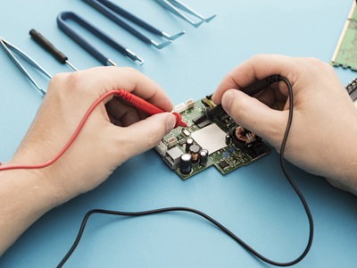
Upon completion of reflow soldering, assembled PCBs undergo rigorous inspection and testing to validate their quality and reliability. Automated optical inspection (AOI) systems are employed to scrutinize the integrity of solder joints, detect defects, and ensure compliance with design specifications. Additionally, functional testing is conducted to verify the electrical performance and functionality of the assembled electronic systems. These inspection and testing processes serve as a final checkpoint, guaranteeing the delivery of high-quality, defect-free electronic products to customers.
6. Final Assembly and Packaging:
With the completion of inspection and testing, assembled PCBs proceed to the final assembly stage, where additional components such as connectors, enclosures, and labels are integrated to complete the electronic system. This stage also encompasses the meticulous packaging of assembled electronic products, ensuring their safe transit and delivery to end-users. From protective enclosures to informative labels, every element of the final assembly and packaging process is meticulously orchestrated to uphold the integrity and functionality of the electronic product.

PCBA assembly stands as a testament to the ingenuity and precision of modern electronics manufacturing. Through a harmonious fusion of advanced technology and skilled craftsmanship, PCBA transforms raw materials into sophisticated electronic systems that power our interconnected world. By exploring the key components and steps of the PCBA process, we gain insight into the intricate mechanisms that underpin the creation of electronic devices, reaffirming the importance of precision, quality, and reliability in the realm of electronic manufacturing. As technology continues to evolve and innovate, PCBA remains at the forefront of progress, driving the advancement of electronic systems that shape the future of our world.
By continuing to use the site you agree to our privacy policy Terms and Conditions.