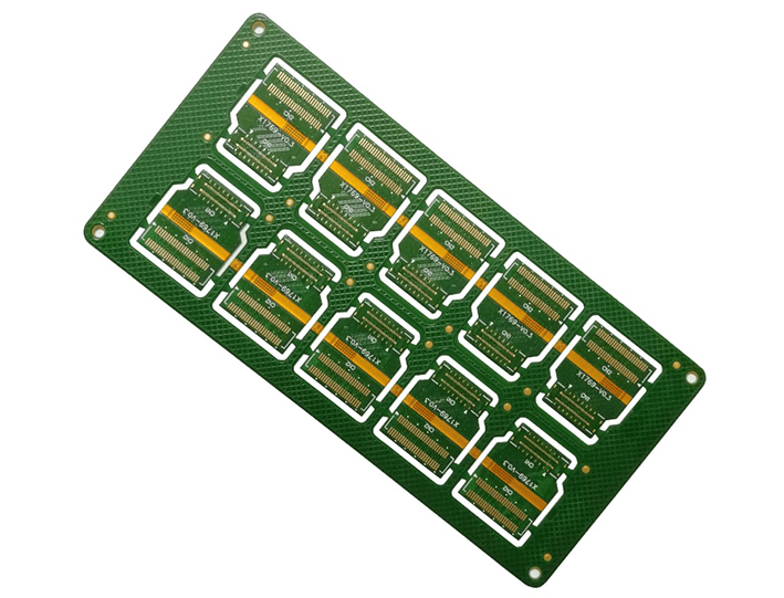
Capabilities Of Rigid Flexible PCB
| PROCESS | ITEM | UNIT | CAPABILITY | ||
|---|---|---|---|---|---|
| Limit Tolerance | Normal Tolerance | Remark | |||
|
Board cutting & thickness |
Layer cutting size: 250mm Min. thickness |
/ mm mm |
2-10 layer 250*1000mm 0.3mm |
2-10 layer 250*500mm 0.3mm |
/ / / |
|
Other auxiliary material |
Adhesive stiffener hot setting adhesive PI stiffener Other stiffener type |
um um um / |
PSA:50um 12.5/25/40um PI: 1.0-13mil steel, Al, silicon steel sheet |
PSA:50um 12.5/25/40um PI: 1.0-13mil / |
/ / / / |
| Drilling |
Min. drilling hole size hole diameter tolerance |
mm mm |
0.1 ±0.075 |
0.2 ±0.1 |
/ / |
| PTH | hole wall copper thickness | um | 8/15/25 | 8/15/25 | / |
| Exposure |
Min line width/space hole ring offset tolerance Line width tolerance Distance between hole edge to outline |
mm mm mm mm mm |
0.05/0.05 0.125 0.1 ±0.03 ≥0.4 |
0.075/0.075 0.2 0.15 ±0.04 ≥0.5 |
/ / / / |
| Lamination |
Coverlay tolerance PI stiffener with outline Sensitive PSA FR4 location tolerance |
mm mm mm mm |
0.15 ±0.3 ±0.3 ±0.3 |
0.2 ±0.3 ±0.3 ±0.3 |
/ / / / |
| Ink |
Soler mask thickness Silk screen thickness |
um um |
8 8 |
15 15 |
/ / |
| R angle for etching cutting die | mm | 0.5 | 0.5 | / | |
| Profile | Steel die tol. |
mm mm |
LS: ±0.075 HS: ±0.01 |
LS: ±0.075 HS: ±0.01 |
/ |
| Cutting die tol. |
mm mm |
Etching: ± 0.20 Wooden: ± 0.30 |
Etching: ± 0.20 Wooden: ± 0.50 |
/ | |
|
Laser tol. Offset tol. for fingers |
mm mm |
± 0.05 ± 0.10 |
± 0.05 ± 0.10 |
/ | |
|
Surface treatment |
Immersion gold | um |
Ni: 2.0~5.0 Au: 0.03~0.08 |
Ni: 2.0~5.0 Au: 0.03~0.08 |
/ |
| Plating tin | um | 8~20 | 8~20 | / | |
Rigid Flexible PCB Production Process
Because of the diversity of the laminated structure and number of layers of the combination of rigid and flexible boards, we will take the four-layer rigid-flexible PCB in the more common single-sided PCB + double-sided FPC + single-sided PCB (1 + 2 + 1) through-hole laminated structure as an example of a simple understanding of the laminated structure, first of all, look at its laminated structure:
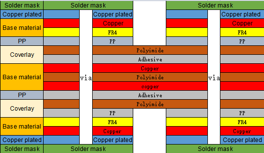
From the laminated structure can be seen, the flexible PCB substrate selection is generally selected without adhesive substrate, mainly to ensure the reliability of the hole metallization and the flexibility of the FPC area, the rigid PCB and flexible PCB bonding adhesive selection of PP to ensure that the bonding force, the flexible area of the solder mask is cover lay , the rigid board area of the solder mask is ink, the following and then take a look at its production process:
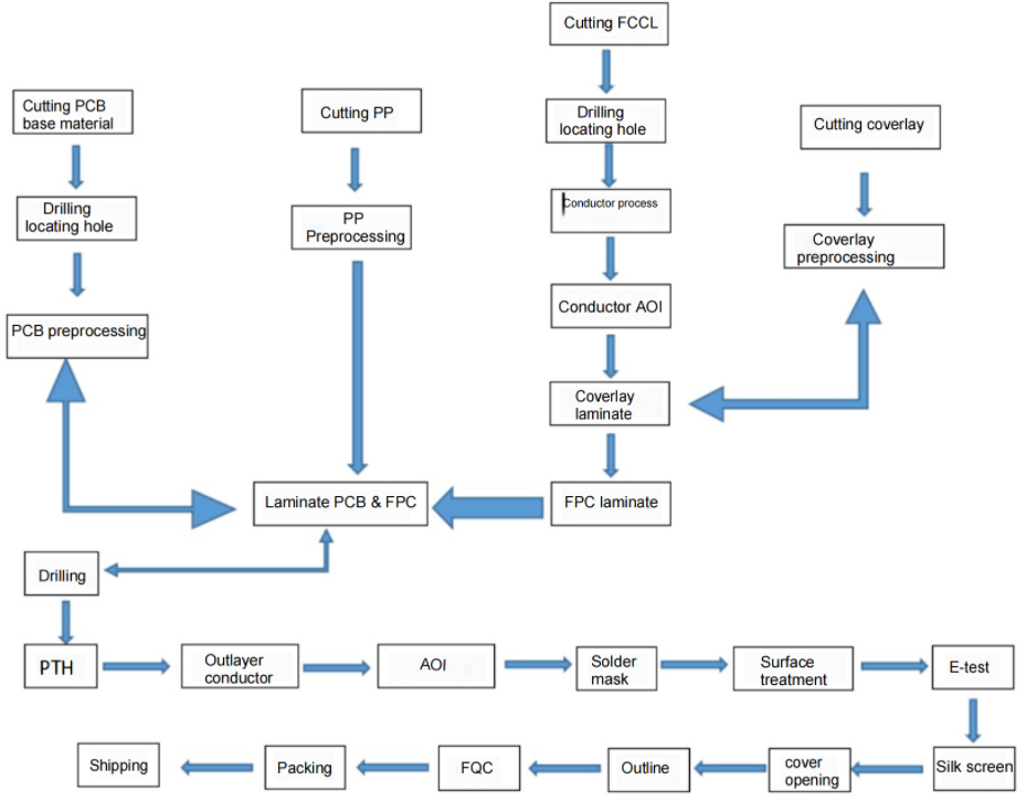
From the production process can be seen in the flexible PCB board substrate and rigid PCB substrate in the pre-processing process before pressing , exactly same with ordinary FPC board production process and rigid PCB board production process .
In the FPC and rigid PCB after the press ing process, looks and conventional double-sided PCB board process is almost the same, the following on a few different processes to be briefly explained:
Rigid flexible PCB pressing
in the high temperature and high pressure will be FPC board and rigid PCB board pressed together, in this process, need to ensure the balance of the thickness of the combination of flexible and rigid board, to avoid the phenomenon of warping . T he main equipment is vacuum compressor;
Cover opening
The purpose is to cut off the top and bottom layers of the rigid PCB board in the flexible board portion of the rigid-flex board, exposing the flexible board in the middle.T he main equipment is laser cutting machine .
AOI
That is, automatic optical inspection, through the optical reflection principle, the image will be transmitted to the equipment processing, and set the information compared to detect the line of open and short-circuit problems, it should be noted that the AOI does not detect the hole copper . T he main equipment is the automatic optical inspection instrument;
Drilling
Drilling positioning holes before pressing flexible and rigid part together , it mainly include drill directional holes, alignment holes, mounting holes, observation holes and ventilation holes, commonly known as first drill, while the flexible and rigid boards are pressed together , there mainly for drilling through holes, commonly known as the second drill .
The main equipment is drilling machine;
PTH
PLATING Through Hole, that is, the meaning of hole metallization, rigid flexible PCB is mainly used in the way of chemical copper plating (immersed copper), this point is different from the ordinary double-sided FPC (black hole) .
The main equipment is PTH lines ;
Outline
Routing + laser cutting , outline for rigid PCB part generally routing edge , while the flexible PCB area shape adopts the way of laser cutting or mould punching .
The main equipment has punching machine, laser cutting machine, routing machine and so on.
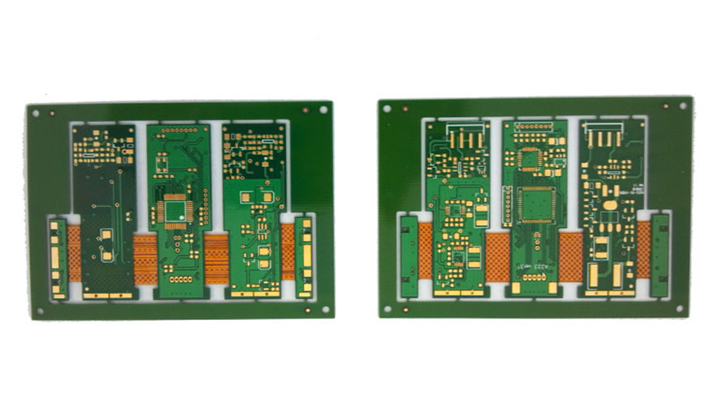
From the above production process, it is easy to see that even the most common 4-layer through-hole , rigid-flexible PCB has more than 30 production processes, the production difficulty is much greater than ordinary single and double-sided FPC, the yield rate will not be very high, the material, manpower, therefore, its price is expensive, the production cycle is longer .
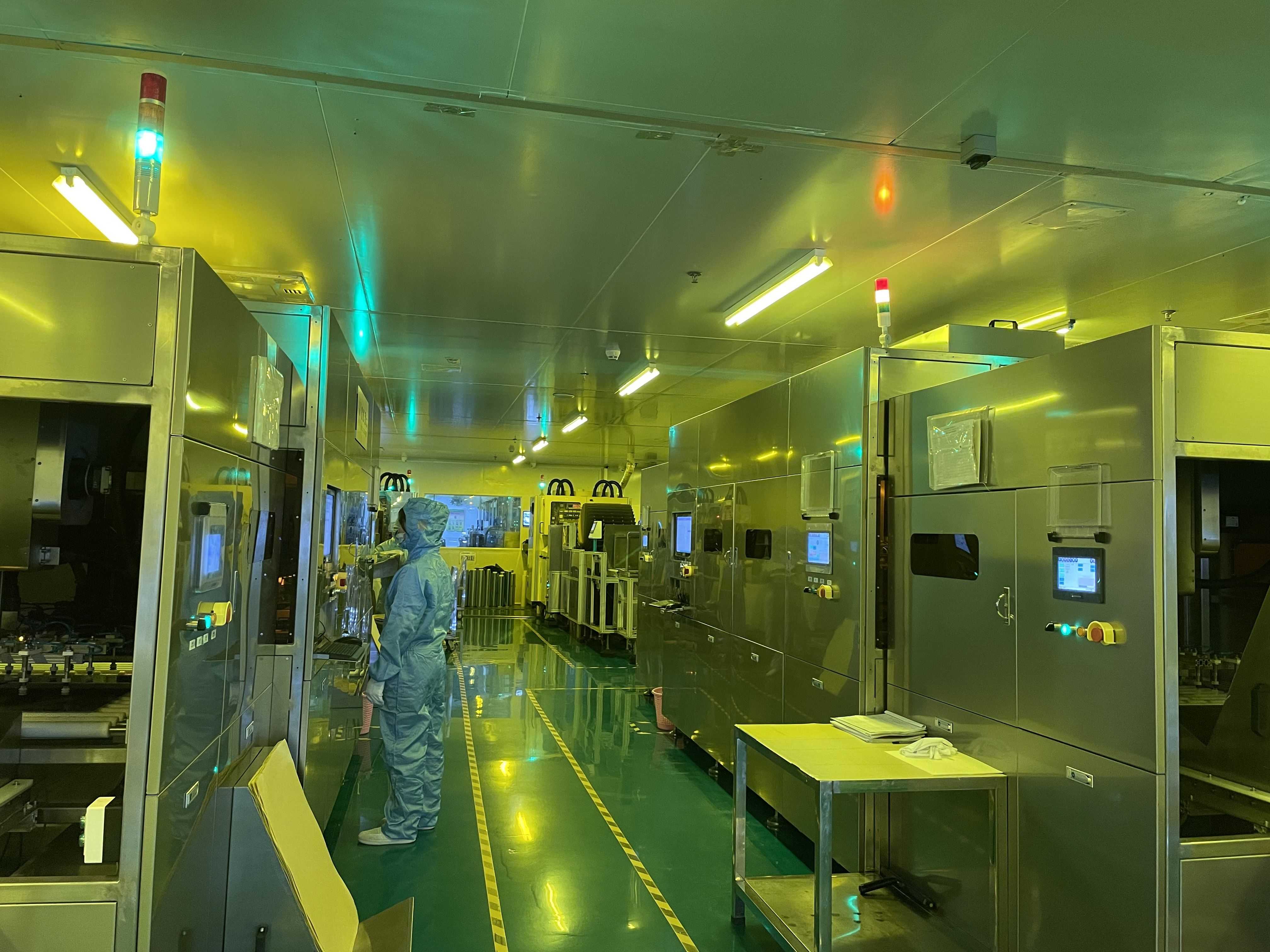
However, SIENTA has high-end production equipment, c omplete quality system, in the field of rigid- flexible PCB board has 20 years of rich technical experience , has the best process experts , has the ability to supply large quantities of high-end Rigid -Flexible PCB board .


