News
Site Editor
 Site
/uploads/image/667d0e0257f45.png
Site
/uploads/image/667d0e0257f45.png
Mastering PCB Export: A Step-by-Step Guide to Creating Gerber Files in Altium Designer
Views: 2011
Author: Site Editor
Publish Time: 2024-06-13
Origin: Site
Exporting a PCB design from Altium Designer to Gerber files involves several steps to ensure that all necessary layers and information are included. Here’s a step-by-step guide to help you through the process:
1.Open Your PCB Project:
Open your Altium Designer software and load the PCB project you want to export.
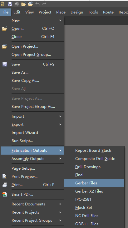
2.Access the Gerber Setup:
Go to
File > Fabrication Outputs > Gerber Files .
 3. Configure Gerber Settings:
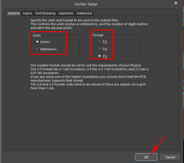
1. General Settings:
1. Set the Units to either Inches or Millimeters.
2. Set the Format to 2: 5
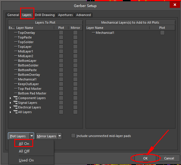
2. Layers Tab:
1. Select the layers you want to include in the Gerber files. Typically, you will select (Double layer) :
1. Top Layer
2. Bottom Layer
3. Top Solder Mask
4. Bottom Solder Mask
5. Top Overlay (Silkscreen)
6. Bottom Overlay (Silkscreen)
7. Mechanical Layers (if used for outlines, etc.)
8. Drill Drawing (for through-hole information)
2. If multilayer PCB , there will be inner layer(G1,G2,G3....)
3. Include the layers that you want to export by marking these, select “Used On” in Plot Layers, Select “All Off” in Mirror Layers.
3. Apertures Tab:
Set the Aperture settings to Auto or Manual as required. Auto is generally sufficient for most designs.
4. Advanced Tab:
Configure any advanced settings, such as plotter settings, if necessary.
4. Generate Drill Files:
1. Before generating the Gerber files, you need to create the drill files.
2. Go to File > Fabrication Outputs > NC Drill Files .
3. Configure the settings in the NC Drill Setup dialog, ensuring that you include plated and non-plated holes, and choose the correct format and units.
4. Click OK to generate the drill files.
5. Generate the Gerber Files:
1. After configuring all settings, click OK in the Gerber Setup dialog.
2. Altium will generate the Gerber files and save them in the specified output directory.
6. Verify Gerber Files:
1. It is crucial to verify the generated Gerber files before sending them to the manufacturer.
2. Use a Gerber viewer (such as the built-in Gerber Viewer in Altium Designer or an external viewer like CAM350 ) to inspect each layer and ensure everything is correctly exported.
7. Zip the Gerber Files:
Once verified, zip all the Gerber files and the drill file into a single archive. This is the package you will send to your
PCB manufacturer.
Summary of Files to Include
Typically, the Gerber package should include:
-
.GTL (Top Layer)
-
.GBL (Bottom Layer)
-
.GTS (Top Solder Mask)
-
.GBS (Bottom Solder Mask)
-
.GTO (Top Silkscreen/Overlay)
-
.GBO (Bottom Silkscreen/Overlay)
-
.TXT or .DRL (Drill File)
-
Any additional mechanical or custom layers
By following these steps, you can successfully export your PCB design from Altium Designer to Gerber files suitable for manufacturing.