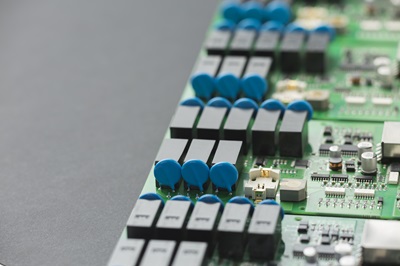
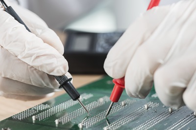
Flexible PCBs (Printed Circuit Boards) are flexible electronic components made from flexible substrates that can accommodate complex three-dimensional spatial layouts. Flexible PCBs play an increasingly important role in modern electronic devices such as smartphones, wearables, medical devices and automotive electronic systems. In this article, we will take an in-depth look at the key steps and challenges of flexible PCB manufacturing.

The first step in flexible PCB manufacturing is to design and layout. Designers need to determine the circuit diagram and layout based on the board's function and application scenarios. Since flexible PCBs can be bent and folded, designers need to consider factors such as the bending radius, the folding method, and the way the board is connected to other components.
Choosing the right substrate and overlay material is critical to the performance of a flexible PCB. Commonly used substrates include polyester films (e.g. Polyester Film), polyimide (PI) films and polytetrafluoroethylene (PTFE). The choice of material also depends on the application scenario and cost factors.
The manufacturing of flexible PCBs usually starts with printing. Printing is the process of transferring circuit diagrams and layouts onto a substrate. Printing can be done using a variety of methods, including screen printing, inkjet, and laser printing. Screen printing is the most common method, which uses a screen to print the pattern onto the substrate and then cures the printed ink through heat treatment or UV exposure.
Electroplating is the process of depositing metal onto the surface of a circuit board. Plating increases the conductivity and corrosion resistance of a circuit board. Plating typically uses metals such as copper, nickel and gold. The process of electroplating includes steps such as cleaning, chemical treatment, plating, and post-processing.
Holemaking is the process of drilling holes in a circuit board. Vias are usually drilled using either mechanical or laser drilling. Mechanical drilling is the most common method, which uses a drill bit to drill holes in the circuit board. Laser drilling is a high-precision method that uses a laser beam to cut holes in the board.
Transfer printing is the process of transferring a pattern from a circuit board to a film. Transfer printing is usually done using either heat transfer or cold transfer methods. Hot transfer is where the board and film are heated together so that the pattern is transferred to the film. Cold transfer involves printing the board and film separately and then using glue to bond them together.
Manufacturing laminates is the process of bonding multiple films together to form a multilayer structure. Laminates are usually made using either the hot press or the press method. Hot pressing involves heating multiple films and copper foils together to bond them. Pressing involves placing multiple films and copper foils together and then using pressure to bond them together.
Fabrication is the process of cutting the laminate into the desired shape and size. Manufacturing the finished product is usually done using either laser cutting or stamping. Laser cutting is a high-precision method that uses a laser beam to cut the desired shape into the laminate. Stamping involves placing the laminate on a press and then using a die to stamp them into the desired shape.
Choosing the right material is critical to the performance of flexible PCBs. However, the characteristics of flexible materials make their processing and handling more complex, such as higher requirements for bending properties, thermal and chemical stability.
Since flexible PCBs typically require higher precision and fine machining, the manufacturing process requires higher precision equipment and process control, which adds to the complexity and cost of manufacturing.
Flexible PCB manufacturing usually requires more processes and more expensive materials, so cost control is a major challenge. Manufacturers need to find cost-effective solutions while ensuring quality.
The design and layout of flexible PCBs require more factors to be considered, such as bending radius, folding method, and connection method, which adds to the complexity and challenge of the design.
Since flexible PCBs may be subjected to bending and flexing during use, their reliability and durability are key concerns in the manufacturing process.
The manufacturing of flexible PCBs requires special equipment and processes, such as laser drilling, hot pressing and stamping, etc. The investment and maintenance of these equipment and processes are also challenges that manufacturers need to face.

The manufacturing process of flexible PCBs involves several critical steps, including design, material selection, printing, plating, holemaking, transfer printing, fabricating laminates, and manufacturing finished products. Manufacturing flexible PCBs requires a high degree of skill and equipment, as well as a number of challenges. However, as technology continues to advance, the manufacturing of flexible PCBs is becoming easier and more reliable, offering more possibilities for the development of electronic devices.
By continuing to use the site you agree to our privacy policy Terms and Conditions.