Technology
Drilling
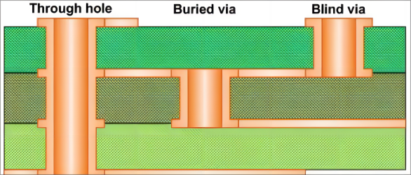
Three common types of drilling VIA holes in rigid or flexible PCB: Throughholes, blind holes, and buried holes
Let's first introduce the meaning and characteristics of these three types of holes in PCB: VIA holes, blind holes, and buried holes.

Through Holes
Definition:
These vias pass through the entire PCB from the top to the bottom layer.Features:
Used for connecting all layers of the PCB.
Easier to manufacture and generally more cost-effective.
Can be used for both signal routing and providing mechanical strength.
Blind Holes
Definition:
These vias connect an outer layer of the PCB to one or more inner layers but do not pass through the entire board.
Features:
Used to increase routing density without taking up space on all layers.
Typically more expensive and complex to manufacture than through-hole vias.
Useful for high-density interconnect (HDI) designs.
Buried Holes
Definition:
These vias connect only inner layers of the PCB and do not extend to the outer layers.
Features:
Invisible from the outer layers, allowing more space for surface components.
Helps to increase layer-to-layer connectivity without using surface area.
Also more expensive and complex to manufacture than through-hole vias.
In the PCB production process, drilling is very important and should not be sloppy.
This is because drilling is the process of drilling the required holes in the laminate to provide electrical connections and hold the devices in place. If the operation is not proper, the process of over-hole problems, the device can not be fixed on top of the board, the light affect the use of the whole board will be scrapped, so the drilling process is quite important.


